Single Crystal Silicon Wafer Fabrication. Wafer thinning is implemented during different process steps as the wafer moves into the manufacturing process flow.
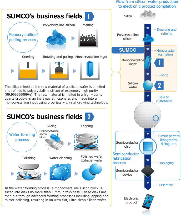
What Is Silicon Wafer Sumco Corporation
Circuit design is traced.

. 3 Process Flow Chart Bonding ASIC. Gold Copper Nickel IndiumTinLead Lead-Free. It is expected that an inspection and test system will prevent killer defects.
Semiconductor Production Process Explained ① Ingot Casting First the sand needs to be. Ad High Quality Roll Chip Bumping Services in North America. CVD Chemical Vapor deposition method to deposit a layer of Si3N4 Hot CVD or LPCVD.
The inspection and test system is incorporated throughout the wafer fab process flow in-line andorend-of-line. Contact 1 was deposited with conventional lithography e-beam evaporation of Nickel-Germanium-Gold-Nickel-Gold 503006003002000 Å and lift. Back EndBE Process Wafer Back Grinding The typical wafer supplied from wafer fab is 600 to 750μm thick.
After the ingot first gets sliced into the individual wafer. Wafer processing is the process of making and obtaining wafers. The silicon wafers so familiar to those of us in the.
UBM 1 UBM 2. Wafer manufacturing process flow 1. Dicing of the Wafer Testing and Inspection of a Single ASIC.
Process flow diagram for the production of semiconductor grade electronic grade silicon. A semiconductor chip is an electric circuit with many components such as transistors and wiring formed on a semiconductor wafer. Wafer thinned down to the required thickness 50um to.
Probe Station and Microscope Etching. Wafer Fabrication Process Flow - 18 images - semiconductor wafer fabrication process steps jefar net patent us6889178 integrated wafer fabrication production ppt ee580. Using granular abrasives eg.
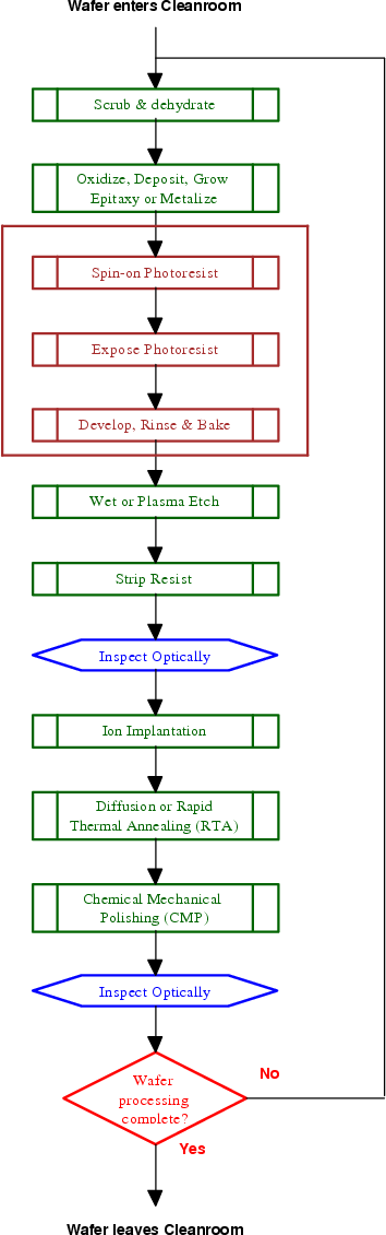
Ad Use Our Wafer Processing Devices For An Efficient Wafer Processing Solution. This chapter will introduce the four basic processes used in the wafer fabrication to form the electrical elements of an integrated circuit in and on the wafer surface. Bumped Diced and.
Enjoy Reliable Support From Our World Class Team Of Experts. Aluminum 50 microns 005 mm of the wafer surface are removed on a. Ad Search Thousands of Catalogs for Wafer Fabrication Process.
The transistor cycle is the basis of. Get A Free Quote Today. The semiconductor manufacturing process flow when highly simplified can be divided into two primary cycles of transistor and interconnect fabrication.
For finishing the surface the wafers pass several process steps.

Die Prep Process Overview Wafer Dies Microelectronic Device Fabrication Packaging
2 5 Fabrication
Improving The Sic Wafer Process Power Electronics News

2 Semiconductor Ic Product Manufacturing Process Flow Download Scientific Diagram


0 Comments